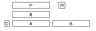
The basic machine has a program counter, P, an index register, X, an accumulator, A, and an auxiliary register, B. There is just one coventional flag register, C, that is used as an overflow flag by arithmetic instructions. A permit interrupt bit may be set and cleared by the programmer.
Various machine options add further registers to the basic set. For instance the high speed arithmetic operation (which adds multiply and divide instructions) makes the shift counter visible, allowing a normalization instruction for floating point work. The high speed option adds a double precision mode allowing the A and B registers to act together as a 31 bit accumulator and allowing double precision addition, subtraction, load and store. A new flag is added recording whether the machine is in double precision mode.
Instruction set
For the details of the standard instructions see table of standard instructions.
In addition to the standard instructions, defined by Honeywell, there are a series of other useful instructions. These are described in a "Technical Memoranda" from the NPL; Micro-coding the DDP-516 computer. This report describes an "Instruction Scan" program to discover the behaviour of one class of instructions, this is recreated here and indentifies one correction to the NPL report.
The series 16 machines have, for the most part, a regular and orthogonal instruction set.
Most instructions are memory referencing instructions. These consist of a four bit code that identifies the instruction, two bits that define the addressing mode (F and T) a "sector" bit, S, and a nine bit address.

| Op code | Mnemonic | Definition | Op code | Mnemonic | Definition |
|---|---|---|---|---|---|
| 0000 | (Generic and shift) | 0001 | JMP | Unconditional Jump | |
| 0010 | LDA | Load A | 0011 | ANA | AND to A |
| 0100 | STA | Store A | 0101 | ERA | Exclusive OR to A |
| 0110 | ADD | Add | 0111 | SUB | Subtract |
| 1000 | JST | Jump and store location | 1001 | CAS | Compare |
| 1010 | IRS | Increment replace and skip | 1011 | IMA | Interchange memory and A |
| 1100 | (Input/Output) | 1101 | LDX STX |
T=1 Load X T=0 Store X |
|
| 1110 | MPY | Multiply | 1111 | DIV | Divide |
Two of the sixteen opcodes are not used for memory referencing instructions. Instead they indicate other classes of instructions, in these two the two bit addressing mode field is reused to distinguish four cases. One non memory-reference opcode indicates IO instructions, in this case the addressing mode field distinguishing the four different IO instructions (OTA, INA, SKS and OCP). The second non memory-reference opcode uses the addressing mode field to distinguish shift, skip, and two classes of "generic" instruction groups.
| FT | Input/Output | Generic and Shift | |
|---|---|---|---|
| 00 | OCP | Output control pulse | Generic control |
| 01 | SKS | Skip if ready line set | Shift group |
| 10 | INA | Input to A | Skip group |
| 11 | OTA | Output from A | Generic arithmetic & half word |
Addressing modes
The standard computer has a maximum memory size of 16K, 16 bit words. With the optional "Extended Memory Addressing" this may be doubled to 32K words. Memory is supplied, at least in the case of the H316 model, in multiples of 4K words.
In order to address the memory it is divided into a series of logical "sectors". Each sector is 512 words.
Any given memory addressing instruction may directly address any word in the current sector (the one in which the instruction is itself located) or in the "base" sector. The base sector is usually (in fact in the vast majority of machines, always) sector zero. The base sector is selected when the sector bit is zero, and the current sector when the sector bit is one.
There is an option, "Memory Lockout Option", that allows the base sector to be relocated to any of the other sectors. This allows for timesharing processes.
Indexing and Indirection
Each memory addressing instruction includes two additional bits; the "Flag" bit that selects indirect addressing and the "Tag" bit that selects indexing. Where both are selected in the same instruction, indexing takes place before indirection.
Indexing causes the contents of te index register, X, to be added to the effective address that is otherwise specified to form a new effective address.
Indirection causes the memory location specified by the current effective address (possibly itself a result of indexing) to be accessed and the value read from that location to be used to form a new effective address. This indirect address can directly address all locations in memory, allowing an instruction to refer to locations other than those in its own sector and the base sector.
The indirect address, itself has a "Flag" and "Tag" bit so that it may call for indexing and/or a further level of indirection. In the standard machine there is no limit to the number of levels of indirection that may be used to form the final effective address.

IO devices
Devices are connected to the processor using an I/O bus. 16 bits are used for data and 10 bits for address. Of these 10 bits six are used to denote the device being addressed, the remaining four defining the function to be performed by the device.
There are four instructions used to control I/O devices.
- INA
- Transfer data from a device to the A register. The data
is ORed into the A register. A device may not transfer all of
the bits. A character device will usually transfer data on
the lower 8 bits (the upper 8 bits of the A
register might contain a character that has previously been
received). If bit 7 of the instruction is set the A
register is cleared before the data is ORed in.
If the device is ready then the next instruction is skipped. If the device is not ready then the data is not ORed into the A register and the next instruction is executed, typically this will be a jump back to the INA instruction causing the computer to wait for data. - OTA
- Transfers data from the A register to the device. If the device is ready then the next instruction is skipped. If the device is not ready then the device will ignore the data on the output bus and the next instruction is executed, typically this will be a jump back to the OTA instruction.
- OCP
- "Output Control Pulse" Is typically used to set the operating mode of the device. The 4 bit function code in the device address is decoded by the device to determine the particular function that the device is to perform.
- SKS
- Tests different conditions (determined by the 4 bit
function code) such as "device ready", "device busy",
etc.
If the particular test is true then the next instruction is skipped.
In addition to the basic programmed I/O instructions, the Series 16 processors provided two alternative high speed I/O schemes:
- DMC
- "Direct Multiplex Control" where data is transfered directly between memory and an I/O device using the standard I/O bus. Transfers are automatically interleaved between instructions. Dedicated memory locations are used to hold the address pointer and buffer end address. Each DMC transfer requires four memory cyles.
- DMA
- "Direct Memory Access" an alternative scheme where a dedicated "DMA" bus is used and data transfers "cycle steal" to effect memory transfers. Unlike DMC, a DMA transfer does not wait for completion of an instruction. A few instructions which are iterative (such as the shifts and multiply and divide instructions) can continue while a DMA cycle is in progress. Dedicated hardware registers and counters are used to hold the address pointer and buffer end address. Each DMA transfer requires just one memory cyle.
The following table shows the various IO devices and their standard device addresses:
| Address | Device |
|---|---|
| '01 | High speed paper tape reader |
| '02 | High speed paper tape punch |
| '03 | Line printer |
| '04 | ASR (teletype) |
| '05 | Card reader |
| '10-'17 | Magnetic tape systems |
| '20 | A pseudo-device used for SMK instructions, Memory Lockout option and Real Time Clock option |
| '22 | Fixed head disk file |
| '23 | Process interface controller |
| '24 | DMA control registers and counters |
| '25 | Moving head disk file |
| '30 | Parallel I/O Channels |
| '33 | Process interface controller interrupts |
| '34 | SKS/OCP Option |